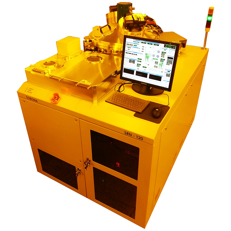
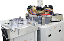
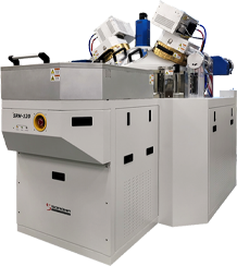
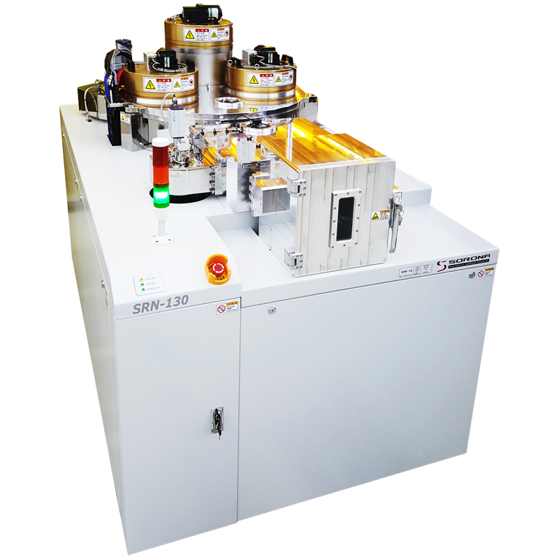
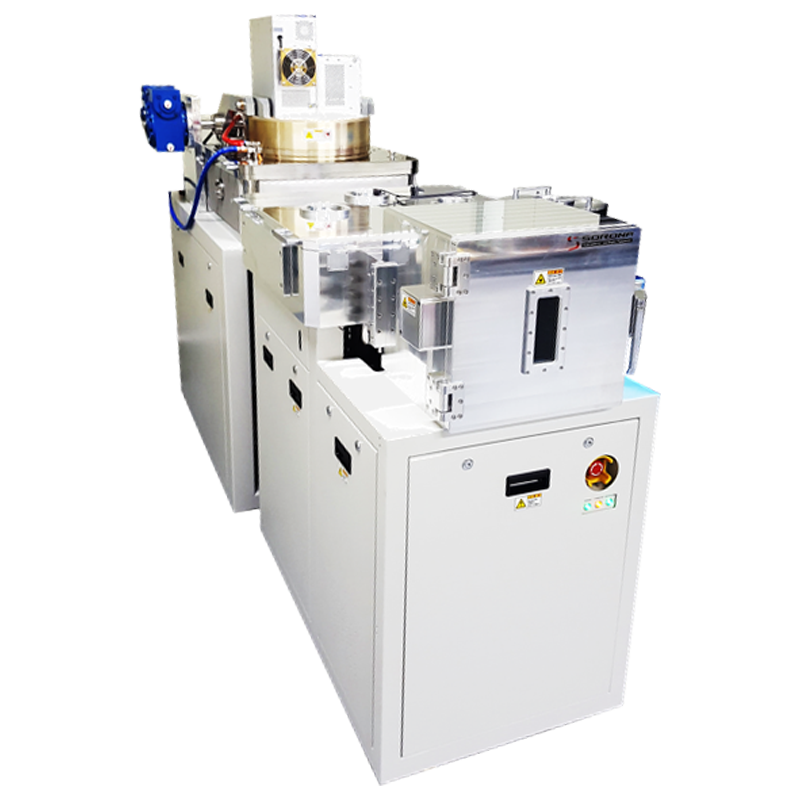
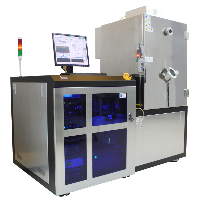
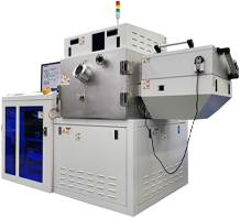
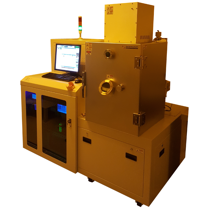
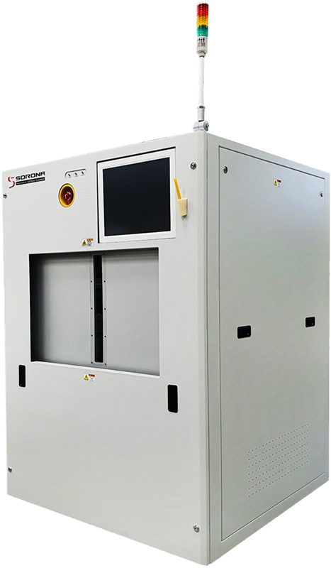
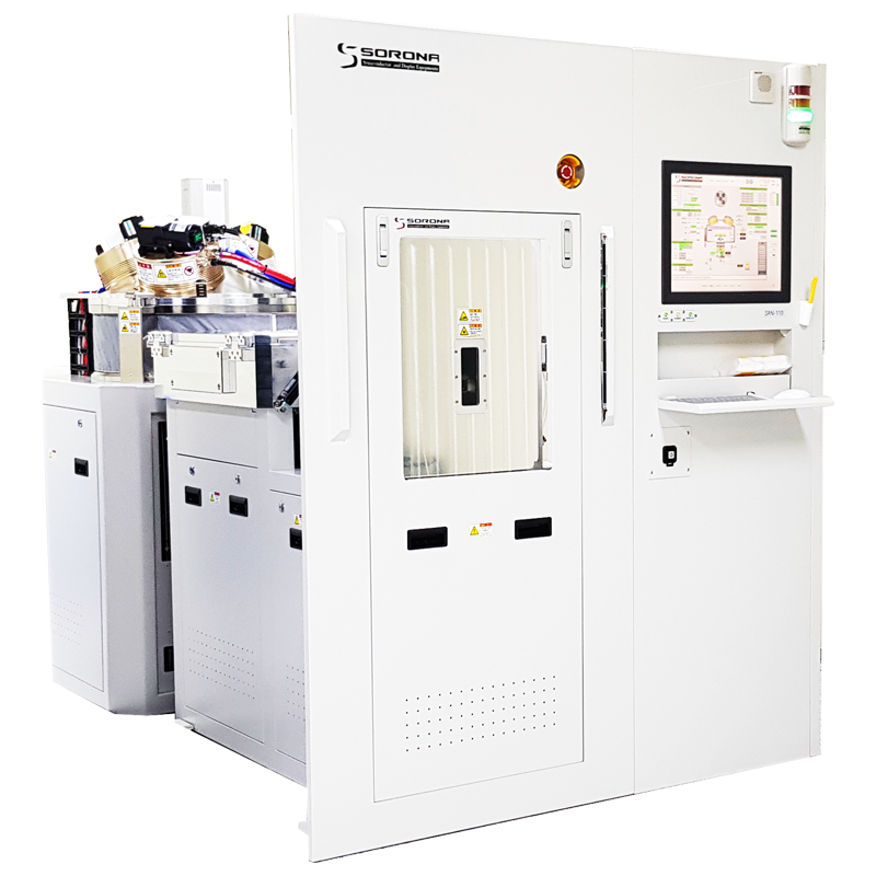
메인 슬라이드 이미지1

Semiconductor sorona

We Make future

메인 슬라이드 이미지2

Display sorona

Dream comes true

메인 슬라이드 이미지3

LED sorona

For human beings

Company

당사는 그동안 축적해온 반도체, 디스플레이 등의 제조공정 기술을 바탕으로 반도체, 디스플레이, LED, MEMS등의 제조에 사용되는 박막증착 및 식각 장비를 생산하는 전문업체입니다.

국내 유수의 반도체 제조업체 및 연구기관에 안정적인 공급을 하고 있고, 기술의 다각화 및 다양한 분야로의 해외시장 진출을 통하여 지속적으로 성장하고 있습니다. 당사는 끊임없는 연구개발과 독자적인 기술개발을 통해 세계최고의 기술력을 갖춘 반도체, FPD 장치분야의 일등기업이 되도록 정진하고 있습니다.

저희 임직원은 항상 변화와 창조적 사고를 바탕으로, 보다 더 나은 제품과 서비스에 초점을 맞춰, 고객의 다양한 요구에 부응하는 제품개발에 총력을 기울여 최고의 가치를 창조하는 파트너가 되겠습니다.

introduction

  • 회 사 명

    (주) 소로나 (SORONA INC.)
  • 대 표 이 사

    윤능구
  • 설 립 년 도

    2004년 12월
  • 주 요 제 품

    Vacuum System Evaporation System Sputtering System PECVD System Reactive Etching System ICP Dry Etching System Vapor SAM Coating System Coating Service
  • Web Site

    www.sorona.co.kr

History

  • 2004

    (주) 소로나 설립
  • 2005

    부설연구소 설립
    ISO9001:2000 품질경영시스템 인증
    벤처기업 인증
    CE 인증
  • 2008

    PECVD System 개발
  • 2009

    중소기업 기술혁신사업 완료
    SAM Coating System 개발
  • 2011

    ICP Dry Etching System 개발
  • 2012

    NASA 협력사 등록 및 공급
  • 2013

    SiGe Epi Growing System 개발
  • 2014

    Microwave Ashing System 개발
  • 2015

    대면적 ICP Dry Etching System 개발
  • 2017

    Plasma Treatment System 개발
  • 2018

    HSC Sputtering System 개발
    In-Line PECVD System 개발
  • 2019

    사옥 이전
  • 2020

    300mm Sputtering System 개발

History

Technology

  • 특허증 이미지
  • 특허증 이미지
  • 특허증 이미지
  • 특허증 이미지
  • 특허증 이미지
  • 특허증 이미지
  • 특허증 이미지
  • 특허증 이미지
  • 특허증 이미지
  • 특허증 이미지
특허증 이미지 특허증 이미지
특허증 이미지 특허증 이미지
특허증 이미지 특허증 이미지
특허증 이미지 특허증 이미지
특허증 이미지 특허증 이미지

Manufacturing

  • SPUTTERING SYSTEM
  • EVAPORATOR
  • ICP ETCHER
  • CVD
  • INLINE PECVD
  • INLINE SPUTTER
  • VAPOR SAM
  • PLASMA TREATMENT
제품 이미지1

cluster sputter

SRN-110

Various purpose deposition/Co-deposition
Unlimited multi layer coating with maximum 12 targets
Protection of the target contamination by intelligent target shield design
Improved convenience of chamber shield exchange
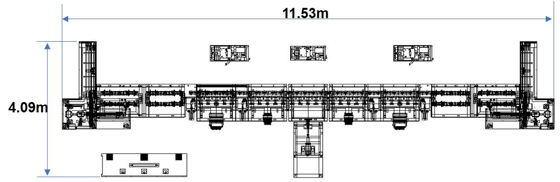
Minimal footprint as compared with quantity of target
Rotating substrate table with RF Bias and heating options

multi-layer sputter

SRN-120

Multi purpose single load-lock sputtering system
4 cathodes with 4inch ~ 10inch target
Available 100mm ~ 300mm wafer deposition
Compact design Available multi-layer coating

제품 이미지2
제품 이미지3

direct sputter

SRN-130

Face to face sputtering
Wafer pre-cleaning stage Available 100mm ~ 200mm wafer deposition
High step coverage module(Optional)
Excellent step coverage performance

reactive sputter

SRN-130r

Face to face reactive sputtering
Available 300mm wafer deposition
Highly quality AlN film growing (FWHM < 300 arcsec)
SAW filter manufacturing MEMS application
Passivation layer coating

제품 이미지4
제품 이미지5
배경이미지

inline sputter

SRN-140

Vertical type INLINE Sputter
Rotary Cathode target
Available 8 generation display
Reactive sputtering(SiO2, Si3N4, TiO2, CrOx)
SiO2 Dep rate > 50Å/min

제품 이미지6

evaporator

SRN-200

Precise single rotating dome design(8inch wafer 5pcs, standard)
Available planetary design optional
Smart shield design(no need screws or clamp pin)
Dome shutter for precision dep rate control Wafer backside heating Max 500℃
Co-evaporation coating or multiple layer
deposition using fully automation software

evaporator

SRN-200i

E-beam & Ion gun combination
Ion beam current support in deposition
Broad divergent beam and excellent uniformity
Low substrate damage control

제품 이미지7
제품 이미지8

icp etcher

SIE-1204

Optimized for PSS and Oxide etching
World leading capacity 12 wafers x 4inch for PSS
No edge exclusion Excellent uniformity
Low particle technology
Outstanding shape control

rie etcher

SRN-300

Single load-lock system
Designed for 100~200mm wafer
Compact dimension & easy operation
Poly-Si, SiO2, Si3N4 and compound semiconductor

제품 이미지9
제품 이미지10

pecvd

SPE-600

SiO2, Si3N4, a-Si Deposition
Minimized footprint
Compact design and High performance
Controllable Reflective index
Controllable film stress

mocvd

Lab scale MOCVD
Metal organic precursor
Atomic layer deposition Chalcogenide compound process
PC control

제품 이미지11
제품 이미지12

vapor sam

AVC-200

Self-Assembled Monolayer deposition
200mm wafer Plasma treatment
Anti-stiction layer deposition
Reactive adhesion layer deposition

vapor sam

AVC-150

Vapor deposited monolayer deposition
Large size 400 x 400 mm deposition
Nano imprint/Lithography stamp coating
Sensor anti-sticking prevention Anti-Fouling barrier

제품 이미지13
제품 이미지14

plasma treatment

PT-600

Powerful plasma treatment and organic cleaning
Electron Free plasma for electronically sensitive samples
600X600mm Tray module
Easy mode change(Active / Ground / Floating)

coating service

Metal coating(Al, Cu, Ti, Tiw, Cr, Ni, Ag, Mo)
Oxide coating(SiO2, Si3N4, ITO, CrOx, TiO2)
Available 3G(550X650mm) sample size

배경이미지
오시는 길

경기도 안성시 원곡면 새울길 9-44

  • 전화 아이콘 Tel 031-667-9954
  • 팩스 아이콘 Fax 031-667-9957
  • 메일 아이콘 sjpark@sorona.co.kr
오시는길 지도